


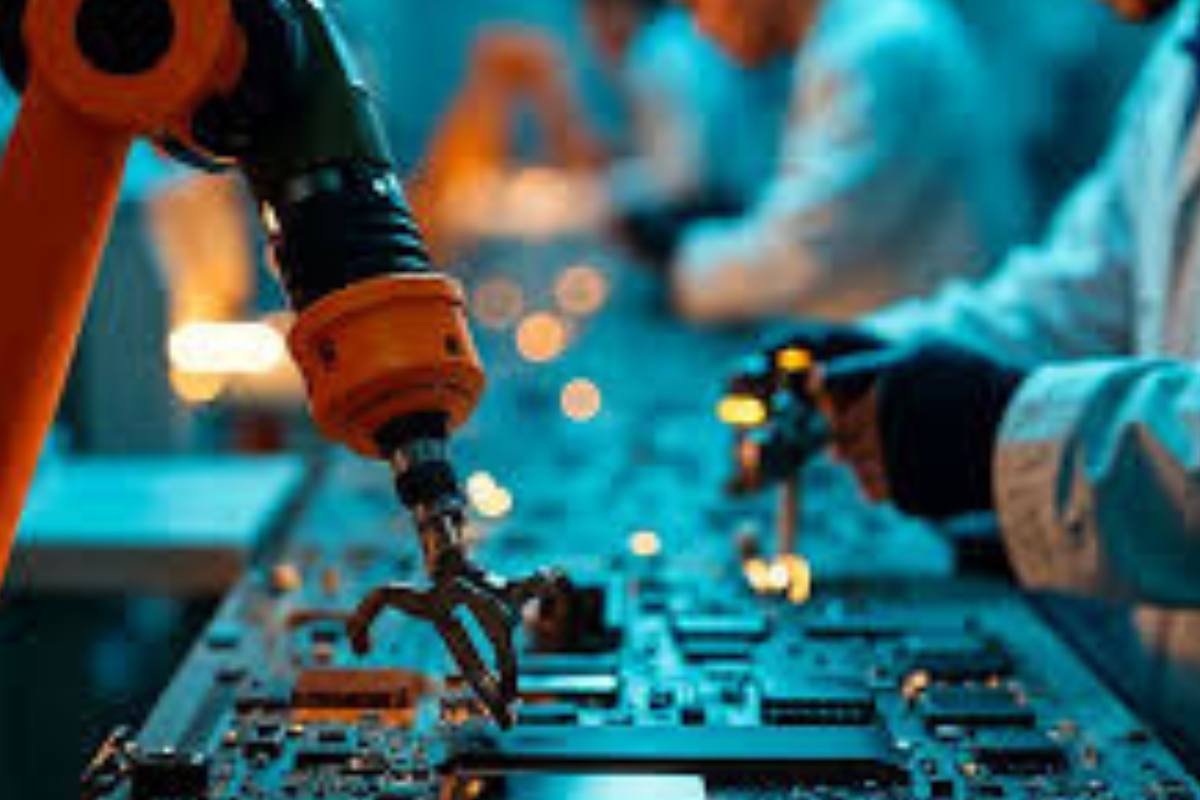
Believe it or not, India’s technology landscape just changed overnight. On August 12, 2025, the Union Cabinet, steered by Prime Minister Narendra Modi, didn’t just rubber-stamp another policy. No, they threw their collective weight behind India’s high-stakes dream: building a robust, homegrown semiconductor industry. Four major projects. Three states, Odisha, Punjab, and Andhra Pradesh. An eye-watering ₹4,600 crore investment. Over 2,000 skilled jobs, for starters. And the ripple effects? Impossible to ignore.
If you’re just catching up: this is about more than just microchips. It’s about India staking a claim in the global technology supply chain, powering everything from electric vehicles and solar inverters to AI servers and next-generation mobile phones. Let’s pull apart the story, layer by layer.
The Fast Facts at a Glance
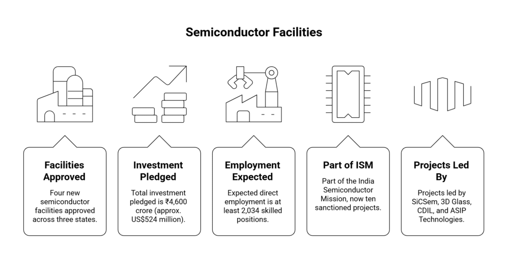
- Four new semiconductor facilities approved, spanning Odisha (2 units), Punjab (1 unit), and Andhra Pradesh (1 unit)
- Total investment pledged: ₹4,600 crore (approx. US$524 million)
- Expected direct employment: At least 2,034 skilled positions; thousands more indirectly
- Part of the India Semiconductor Mission (ISM): Now a total of ten sanctioned projects, worth more than ₹1.60 lakh crore, dotting six states
- Projects led by: SiCSem Pvt Ltd (with UK’s Clas-SiC Wafer Fab), 3D Glass Solutions Inc., Continental Device India Ltd (CDIL), and Advanced System in Package (ASIP) Technologies (with South Korea’s APACT Co., Ltd.)
Funny thing is, it’s not just about setting up factories. It’s a leap towards a self-reliant (Atmanirbhar) India in electronics, a sector that, until recently, seemed out of reach.
A Closer Look at the Key Semiconductor Plant
Let’s start where two of the four projects are landing: Odisha, specifically Bhubaneswar’s bustling Info Valley.
SiCSem & Clas-SiC Wafer Fab Pvt Ltd. (UK): India’s First Commercial Silicon Carbide Fab
Picture it: a cutting-edge facility cranking out 60,000 silicon carbide wafers per year, plus 96 million packaged units annually. That’s no ordinary feat.
- Technology: Silicon carbide (SiC) chips, sought after for high-voltage, high-temperature electronics
- Applications: Defense systems, electric vehicles, railway traction, solar inverters, and advanced consumer appliances
- Why SiC Matters: SiC semiconductors deliver better efficiency and performance in tough conditions, hot, high-voltage environments, where ordinary silicon can’t cope.
3D Glass Solutions Inc.: Advanced Packaging for Next-Gen Devices
The second project in Odisha? It’s all about the packaging, the invisible backbone that makes modern chips tick.
- Core tech: Vertically integrated advanced packaging, embedded glass substrates, and 3D Heterogeneous Integration (3DHI) modules
- Annual capacity: 69,600 glass panel substrates, 50 million assembled units, and 13,200 3DHI modules
- Industry reach: Computing, AI, defense, automotive, photonics, plus high-performance computing
- Edge: The facility brings world-class glass-based packaging tech to India, a crucial upgrade for everything from smartphones to servers.
You might wonder, why glass? Turns out, glass substrates offer better speed, lower power consumption, and greater package miniaturization, just what edge-computing and AI chips desperately need.
Punjab: Mohali’s CDIL Poised for Expansion
Let’s zip north to Punjab, where Continental Device India Ltd (CDIL), a seasoned player in Indian semiconductors, just got a shot in the arm.
- Expansion: Brownfield upgrade for Mohali’s discrete semiconductor facility
- Tech focus: MOSFETs, IGBTs (think: electric vehicles and renewable energy), Schottky bypass diodes, and power transistors, using both traditional silicon and advanced silicon carbide
- Annual production: Projected at 158.38 million units
- Market impact: Automotive, renewable energies, industrial controls, power conversion, and the country’s growing communication infrastructure all get a big lift here.
For context: “brownfield” means they’re expanding on an existing footprint, so the learning curve (and the downtime) is shorter.
Andhra Pradesh: ASIP and APACT, Packaging the Future
Down south in Andhra Pradesh, Advanced System in Package Technologies (ASIP) is partnering with South Korea’s APACT Co., Ltd., a major name in semiconductor packaging and testing.
- Facility output: 96 million units per year
- Product range: System-in-package solutions for mobile phones, set-top boxes, automotive electronics, and broader consumer markets
- Global twist: APACT brings experience and technical depth, nudging India closer to the world leaders in semiconductor packaging.
If I’m honest, this is where global collaborations start to pay off. Indian know-how, overseas technical expertise, and an environment where both can thrive.
Why This Surge in Semiconductor Investment, And Why Now?
Here’s the kicker: India’s electronics market is expanding at a breakneck pace. Every EV, every AI-enabled gadget, every 5G antenna, that’s more semiconductors needed. But, until now, India imported most of its chips, vulnerable to global supply shocks and bottlenecks.
- Sectors demanding chips: Telecom, automotive, defense, high-performance computing, data centers, consumer appliances, and industrial equipment. It’s an endless list
- Global context: Chip shortages (remember those pandemic supply chain nightmares?) laid bare just how critical, and how fragile, supply chains could be.
- Self-Reliance: These projects will help India slash its dependence on imported semiconductors. That’s a big deal for national security, economic resilience, and even job creation.
The India Semiconductor Mission: Bigger Picture
Now, ISM isn’t just about dropping a few billion on factories; it’s a coordinated government push with an eye on the future. Here’s how it stacks up, as of August 2025:
- Total semiconductor projects sanctioned: 10 (including these 4), spread across 6 states
- Total capital committed: Over ₹1.60 lakh crore (approx. US$18.23 billion)
- Covered regions: Gujarat, Assam, Uttar Pradesh, Odisha, Punjab, Andhra Pradesh
- Design Infrastructure Support: Extended to 278 academic institutions, 72 startups, and counting
And it’s no accident. The government is offering cost subsidies, performance-linked incentives, and crucially, a design push to foster local chip startups and academic research
Talent Pipeline: Jobs and Skills, on the Rise
You might say: factories are great, but who’s going to run them? Turns out, there’s an answer.
- Direct jobs: Official estimates peg it at 2,034 new skilled positions (just for these four projects)
- Indirect jobs: Thousands more, think: supply chain, maintenance, logistics, local ancillary units
- Skills focus: From engineers and chip designers to packaging specialists and machine operators, it’s an all-hands-on-deck moment. Over 60,000 students have already been trained through new industry-aligned curricula.
In other words: this isn’t just about “shrinking unemployment.” It’s about building a talent pool that can keep up with global industry standards.
Breaking Down the Four Projects
Let’s make things crystal clear. Here’s a snapshot of the who/what/where:
| Project & Collaboration | Location | Focus Area | Annual Output | Applications |
| SiCSem + Clas-SiC Wafer Fab (UK) | Bhubaneswar, Odisha | First Silicon Carbide fab (compound semiconductors) | 60,000 wafers; 96M packaged units | Defense, EVs, Railways, Solar |
| 3D Glass Solutions Inc | Bhubaneswar, Odisha | Glass-based advanced packaging & substrates | 69,600 glass panels; 50M assembled units; 13,200 3DHI modules | HPC, AI, Defense, Photonics |
| CDIL | Mohali, Punjab | Expansion (power discrete semiconductors: MOSFETs, IGBT, etc.) | 158.38M units | Autos, Renewable energy, Industrial |
| ASIP + APACT (South Korea) | Andhra Pradesh | Semiconductor packaging for mobile, auto, and devices | 96M units | Mobile, Set-top, Auto electronics |
Government’s Incentives: Real Money on the Table
One, India’s government isn’t leaving it to chance. Besides the ISM initiative:
- Design-linked incentives: Up to 50% for design/prototyping costs (max ₹15 crore per chip design)
- Performance-linked incentives: 4–6% on net chip sales over five years (capped at ₹30 crore per design)
- Fast-track clearances: Recent projects, sources say, were greenlit within 100 days, with some construction work launching in six months.
Innovation, Academic & Startup Synergy
Here’s a subtle shift: it’s not just big factories. Between academic grants (278 institutions), startup funding (72 companies), and successful prototype designs, India is seeding tomorrow’s chip design workforce.
In July 2025 alone, 23 chip design projects received the Ministry of Electronics & IT’s nod. Focus areas? Everything from surveillance systems to microprocessor IP cores.
- Spin-off: 10 startups have snared venture capital; six companies sent “tape-outs” (chip blueprints) to international foundries; 17 institutions completed 20 chip designs at India’s own Mohali lab.
A clever move, by investing in both “chip making” and “chip designing,” India is laying the foundation for a full-stack semiconductor ecosystem.
Turning the Tide: Strategic and Economic Impacts
Consider the bigger, more strategic canvas:
- National security: When critical defense and communications tech depends on imported chips, vulnerabilities multiply. Domestic fabs mean tighter control and better resilience.
- Global competitiveness: By mastering advanced packaging, glass substrates, and global partnerships, India is muscling into tech territory once monopolized by East Asia and the U.S.
- Supply chain stability: No more “chip shortage” shutdowns for Indian manufacturers, cars, devices, and energy converters. That means smoother, more predictable industrial output.
And, naturally, this aligns with the “Make in India” push, reducing reliance on overseas supply, boosting high-value exports, and spurring economic growth.
Cross-Border Partnerships: Why Foreign Players Matter
One thing that stands out? Nearly every project involves international technology transfer or a joint venture.
- UK’s Clas-SiC Wafer Fab: Know-how for SiC fabrication, critical for India’s first-ever compound fab.
- South Korea’s APACT Co., Ltd.: World-class packaging techniques, giving India a shot at advanced system-in-package production.
These partnerships mean India leapfrogs past some painful “learning curve” years, absorbing global best practices and shortening its runway to full-scale production.
Challenges on the Horizon, And How India is Tackling Them
Now, no one’s saying this will be easy. The semiconductor game is tough.
- Capital intensity: Setting up a modern fab costs billions; one mistake, and you fall behind rapidly evolving tech.
- Skill shortage: Even with the government’s training blitz, talent wars are real. Countries worldwide are scrambling for chip engineers.
- Supply chain dependencies: Raw materials like ultra-pure silicon, specialty gases, and even equipment still rely on global suppliers. Decoupling won’t happen overnight.
- Market competition: China, the U.S., Taiwan, South Korea, they’re not sitting still.
But the boldness of these new projects, backed by government guarantees, fast-track policies, and international tie-ups, is giving India momentum it’s never had before.
Voices from the Ground, Comments and Commitments
Just hours after the approval, both the Chief Ministers of Odisha and Andhra Pradesh publicly thanked the Prime Minister, vowing to expedite construction and clear local bottlenecks. Union Minister Ashwini Vaishnaw, for his part, stressed that the four new plants would “start their design and build-out in record time,” echoing the brisk progress of earlier ISM projects.
Construction, if recent timelines hold, could kick off within six months, an unusually fast gestation period for such complex ventures.
Looking Ahead: The Future of Indian Semiconductors
There’s no denying it: these four projects don’t just add new pins to India’s tech map, they change the conversation. For students, engineers, entrepreneurs, and factory hands alike, the opportunities are multiplying. For India’s vast and growing consumer base, the promise of “Designed and Made in India” semiconductors in everyday devices comes tantalizingly close.
And for government planners, the blueprint is now in place: nurture the design ecosystem, pair it with state-of-the-art manufacturing, draw on global partners, and scale up, fast.
Key Takeaways
- India is shifting from semiconductor importer to emerging heavy-hitter, thanks to targeted policy and high-impact investment.
- Four new projects, across Odisha, Punjab, and Andhra Pradesh, will anchor India’s next wave of electronics manufacturing.
- Strategic international collaborations are accelerating technology transfer, skills growth, and best-practices rollout.
- The India Semiconductor Mission is more than a funding source: it’s a signal of long-term commitment, cross-sector innovation, and relentless focus on supply chain resilience.